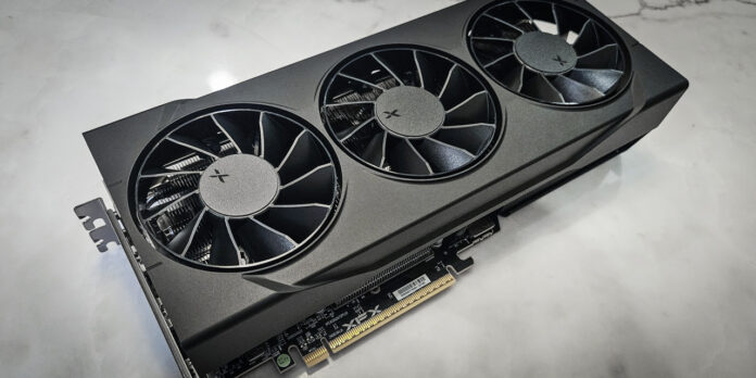
The basis of 9060 XT is a chip code named Navi 44. This is essentially ½ of a Navi 48, which powers the RX 9070 series. It is a 29.7 billion transistor chip with a die size of approximately 199 mm square. It is produced on TSMC’s N4P node. It features 2048 shading units, 128 TMUs, 64 ROPs, 32 RT cores, 32 compute units, and a 128-bit memory controller. Higher end 9060 XT boards will consume upwards of 180 watts of power (and likely more). It does not quite scale down to half the actual size of the Navi48, but that is due to other common structures such as the decode engines remaining in the same number of units and sizes.
The 128-bit memory bus is paired with 20 Gbps GDDR6, giving it around 320 GB/sec of memory bandwidth. Each chip also features 4 MB of L2 cache and 32 MB of L3 cache. This does take some of the burden off of the smaller memory bus to achieve better overall throughput in modern graphics applications.
The RDNA 4 architecture is a clean sheet design that borrows some things from previous generations, but advances the entire family with redesigned RT units as well as dedicated AI Acceleration Cores (NVIDIA uses the term Tensor Cores). It also features a significant improvement in overall power efficiency from the RX 7000 series. For example it achieves a 30% increase in performance vs. the RX 7600 XT while actually consuming less power than that older 6nm product.
AMD truly has a competitive architecture to throw at NVIDIA in 2025. So far their products have compared well with the competition, all the while being slightly less money at every level of performance.

